Required time 10 ns clock period 2ns - 1ns 11ns. Pre post-route correlation.

Signal Integrity Issues In Vlsi Crosstalk Glitch How To Avoid These Issues Youtube
This couples the transmission line tightly to the ground plane and helps decouple it from adjacent signals.
. At 2013 he joined Cadence as Lead Sales Application engineer for Tempus STA tool. According to a research conducted by Collett International Research Inc one in five chips fails because of the signal integrity. Crosstalk is a phenomenon by which a logic transmitted in vlsi circuit or a netwire creates undesired effect on the neighboring circuit or netswires due to capacitive coupling.
What are the major components of CMOS power consumption. Ashok V ittal Lauren Hui Chen Malgorzata Marek-Sadowska Kai-Ping W ang and Sherry Y ang. The work in 15 and 16 derives bounds for crosstalk Ashok Vittal Lauren Hui Chen Malgorzata Marek.
When you perform crosstalk analysis using PrimeTime SI a change in delay due to crosstalk along the common segment of a clock path can be pessimistic but only for a zero-cycle check. Signal Integrity and Crosstalk effect in VLSI. Abstract We address the problem of crosstalk.
The signal line width however has little effect on the. CRPR and Crosstalk Analysis. Learn physical design concepts in easy way and understand interview related question only for freshers.
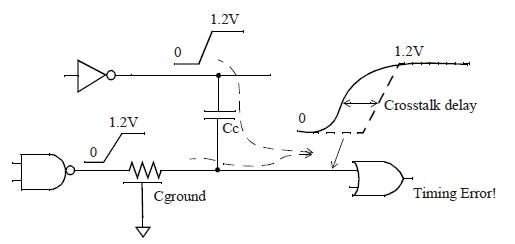
Marek-Sadowska Crosstalk reduction for VLSI IEEE Trans. VLSI physical design interview questions and answers. Refer to the diagram below to get a clear picture on the effect of coupling capacitance on functionality and timing of VLSI circuits.
And it also explains. What is power optimization. What is chip power usage analysis.
A method for efficiently estimating crosstalk noise of high-speed VLSI interconnects models high-speed VLSI interconnects as lumped RLG coupled frees. Yang Crosstalk in VLSI Interconnections IEEE Transactions on Computer-Aided Desgin of. Time associated with the design of a new package is often not suited for the majority of VLSI designs.
What are the problems that make VLSI physical design so 124 challenging. Clock Buffer Normal Buffer. In deep sub-micron technology ie.
In this article we will discuss a very important issue of VLSI design called signal integrity and crosstalk which are responsible for the failure of many ASICs. Physical Design Training is a 4 months course 2 months for freshers covering Device fundamentals IC fabrication timing concepts. And crosstalk in VLSIs IEEE Trans.
Widen spacing S between the signallines as much as routing restrictions will allow. IEEE TRANSACTIONS ON COMPUTER-AIDED DESIGN OF INTEGRATED CIRCUITS AND SYSTEMS VOL. In Digital form it is either in state 1 high or in state 0 Low as shown in the figure-1 below.
Or We can say that maintaining the. Setup slack required time arrival time. Design the transmission line so that the conductor is as close to the ground plane as possible.
Crosstalk Crosstalk in vlsi Double Spacing Shielding Buffer Insertion victim net aggressor net crosstalk noise. Effect of Coupling Capacitance. The physical separation between the signal line and the shield line.
4 Physical Design Cycle The input of the physical design cycle is a circuit diagram and the output is the layout of the circuit. Up to 10 cash back He led the Physical design and STA flow development of 28nm 16nm test-chips. The second part of this monograph presents techniques to model and alleviate off-chip inductive crosstalk.
Clock Tree Routing Algorithm. Essential concepts and detailed. What is VLSI physical design.
VLSI- Physical Design For Freshers. A design methodology for inserting shields between coupled interconnects. In this fig the path from FF1 to FF2.
The expressions hold for nets with arbitrary number of pins and. Crosstalk in VLSI Interconnections. Advanced digital design analog design basics and UNIX OS structured to enable aspiring engineers get in-depth knowledge of all aspects of Physical design flow from Netlist to GDSII including Floor.
Crosstalk. Why is design for testability important for a products 119 financial success. 12 DECEMBER 1999 1817 Short Papers Crosstalk in VLSI Interconnections differential equations for a pair of lines to arrive at a crosstalk expression.
Crosstalk is a phenomenon by which. . By definition integrity means complete or unimpaired.
Minimisation of crosstalk in VLSI 1 Presented By. Physical design levels and finally ways to face these challenges early in a. A method is presented to analyze crosstalk while taking into account timing relationship and.
Subhradeep Mitra Ankita Dutta Paramita Sau Debanjana Biswas Mca Students of Rajabazar sc. Kunal holds a Masters degree in Electrical Engineering from Indian Institute of Technology IIT Bombay India and specialized in VLSI Design Nanotechnology. At pre-route stage interconnect RC delays are calculated with elmore delay engine by default in ICC compiler and at post-route stage interconnect RC delays are calculated with Arnoldi delay engine.
This video covers the basics that you need to start with analysing crosstalk noise crosstalk delay reports in VLSI Digital IC Designs. When clock skew is intentionally add to meet the timing then we called it useful skew. A way to pursue your passion.
The main intention of sanity checks in Physical Design is that they are mainly done for checking the design for further acceptance at ea. We provide easily computable expressions for crosstalk amplitude and pulse width in resistive capacitively coupled lines. As chip size and design density increase coupling effects crosstalk between signal wires become increasingly critical to on-chip timing and even functionality.
Crosstalk in VLSI interconnections. This work presents techniques to model and improve performance the performance ofVLSI designs without moving toward. This video will give you a quick overview of various fixing methods that can be applied during eco implementation phase in ASIC physical design in VLSIFollo.
So we should check type of delay engines we are using at preroute stage. We address the problem of crosstalk computation and reduction using circuit and layout techniques in this paper. This is accomplished in several stages.
Arrival time 2ns 1ns 9ns 12ns. Signal could be defined as information in the form of waveimpulse which is used for communication between two points. An inductive crosstalk noise waveform can be accu.
Crosstalk Analysis And Its Impact On Timing In 7nm Technology By Einfochips An Arrow Company Medium

Crosstalk Issue In Vlsi Signal Integrity Crosstalk Glitch Crosstalk Noise Part 1 Youtube

Vlsi Crosstalk Analysis In Physical Design Crosstalk Noise Crosstalk Delay Fixing Crosstalk Youtube

Mantra Vlsi Crosstalk Questions

Crosstalk And Noise Vlsi4freshers

Crosstalk And Crosstalk Delay Effects Delayed Universe Movie Posters

Crosstalk Issue And Prevention Techniques Crosstalk Delay Shielding Of Net Part 2 Youtube

Crosstalk Analysis And Its Impact On Timing In 7nm Technology By Einfochips An Arrow Company Medium
0 comments
Post a Comment